HeaterMeter Noob - Is it hard to build?


Atmega socket is fine, as long as you put the chip in correctly with the half moon towards the edge.

The shift registers half moon needs to be towards the .1 cap and yes to the right
 
If by chance you do put the atmega in backwards, nothing will happen. It wont get programmed, and you can just reverse it to the correct position and all would be ok.
 
That has been done before. The problem is that desoldering is a bear especially for a multi pin component such as this. I know there are a couple threads about attempted corrections and I don't think they were successful. Hopefully somebody that was able to do this will chime in. But since nobody has yet, you might want to try getting some de soldering braid and get out as much solder as possible then get some of this:

http://www.amazon.com/exec/obidos/ASIN/B0019UZP7I/tvwb-20

Watch a few videos about ChipQuik and see if it's something you want to try. I bought some and have played with it and it really does work as advertised but removing the LCD is still a daunting task.

Good Luck!

Once again, hopefully someone will chime in that has successfully removed a LCD.
 
Last edited:
I've done it, but did hose up one trace on the LCD in the process, which I fixed with a jumper wire... so all good. Not the easiest thing to do but it can be done..
 
Its not easy to remove the LCD and like what Ralph said, the pads may get damaged. The first thing to do if you can is to remove each pin one at a time. Get some tweezers and heat each pin and pull it out. Next take some solder braid and some Flux, dip the briad in the flux and apply some on the Lcd pads. Apply the braid to the LCD pads and then the soldering iron. Don't leave it on there to long, let it cool and re-apply. You can also use a solder Sucker to try to get more of the solder out. Also do the Heatermeter pads. After get most of the solder out, depending on how much solder you started with, the solder may be in-between the lcd and the Heatermeter. There is not much you can do to remove that solder in-between.

Now, you can get some thin gauge wire and loop it through the LCD and the Heatermeter weaving it up and down through all 12 solder points, don't weave the wire tight, leave some slack so that the LCD and the Heatermeter can be pulled apart. This has no guarantees working as I thought of this Idea just before writing this post, lol. But the idea is to heat up the wire with the soldering iron and as it heats up it will gradually heat each solder pad and hopefully it will give you enough time to remove the LCD from the Heatermeter. The Idea is to heat all the pads at the same time so that the solder does not hold the LCD to the Heatmeter.

I have removed a few LCDs and they are not easy maybe a 20%-30% chance at saving it and even lower percentage of saving all the solder pads.
 
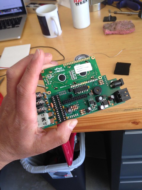
This was my first PCB, so thought I'd share some images of the project and some feedback. First of all, the instructions were unparalleled. Better than most things I've purchased. There were a couple spots where the resistor housings (not stripes!) were different colors, etc. but that's to be expected.

* the helping hands were less necessary than I thought. I could have done the whole thing without them.
* a small soldering tip and small soldering wire were very helpful
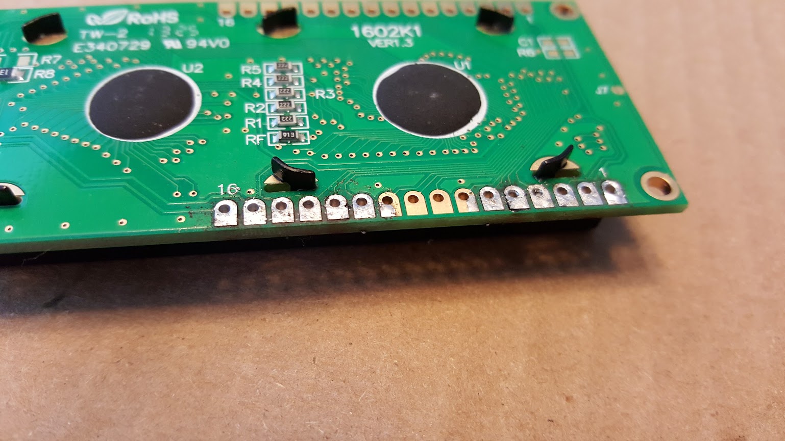
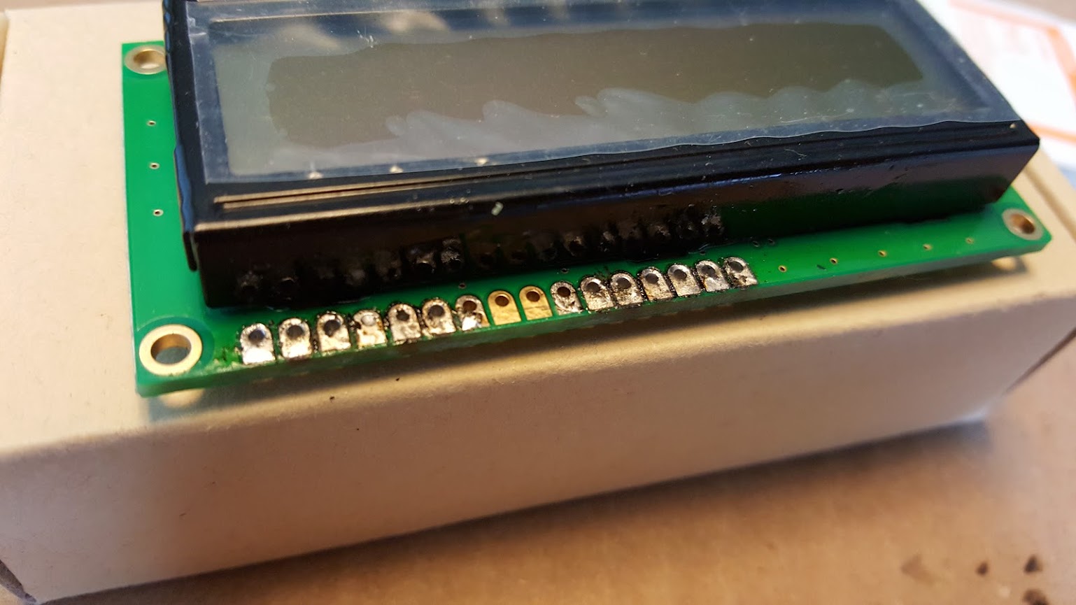
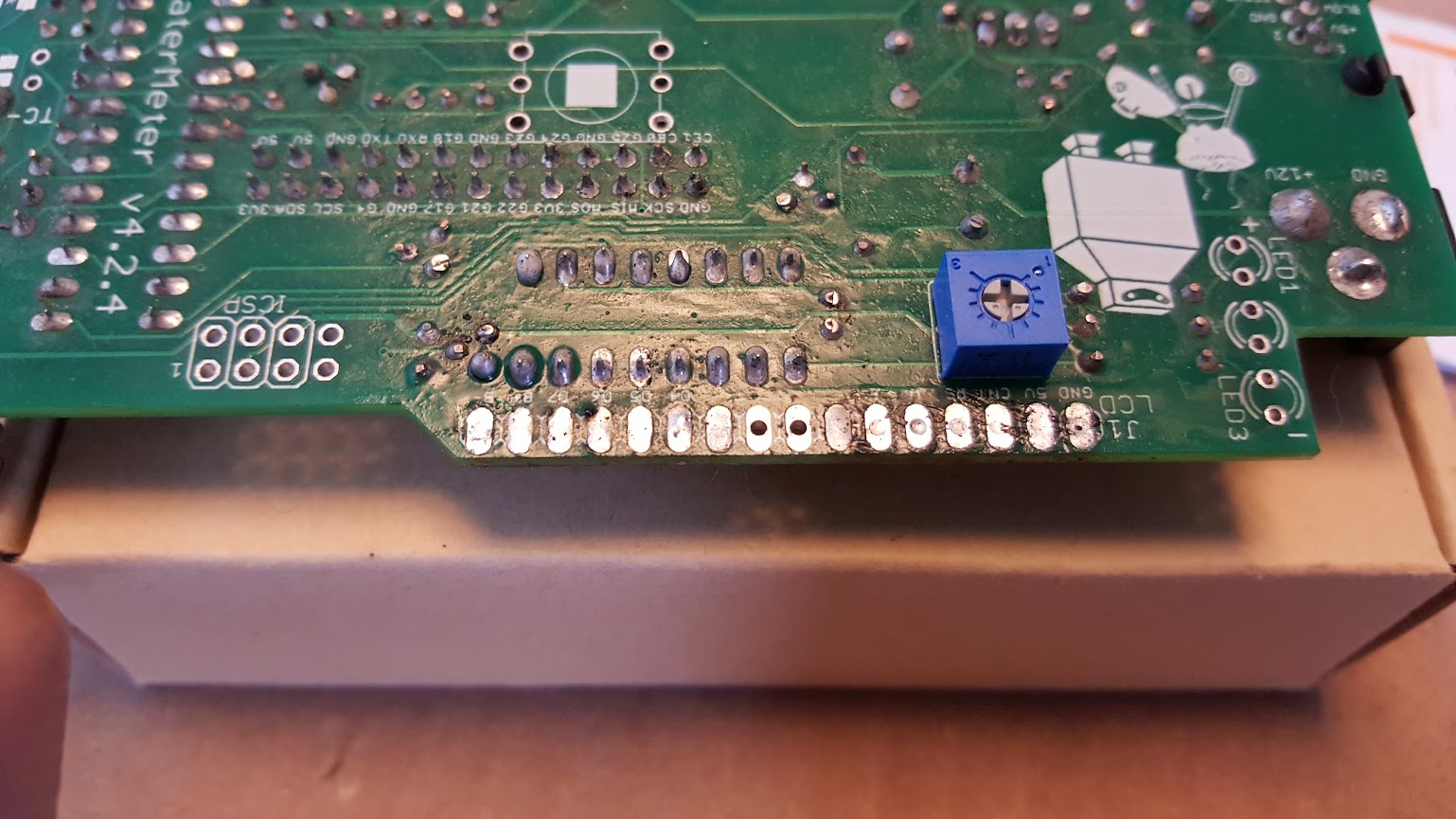
* some of the PCB solder points spilled over to holes right next door--the board was designed for this, but a little diagram of "where this is ok, and where it's the end of the world" would have made me feel a little bit better
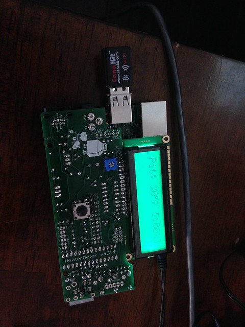
* The LCD step-by-steps were perfect. That said, my pattern for reading directions/doing was pretty solid for a NOOB and I still made 2 mistakes.

Here was my process. All in, I'd guess I spent 4-5 hours soldering and the "extra steps" took a total of 45 minutes on top--well worth it to remove NOOB risk:
1. Read all the directions through even the parts that aren't necessary--e.g., I read about the Raspberry Pi A even though I used a B (15 minutes)
2. Do one section (1-2 steps at a time). Read the 1-2 steps before, those 2 steps and then the 2 steps afterwards. If I'm starting after a break, skim all of the instructions again to re-orient.
3. Have the laptop about 1.5 feet away at all times (close enough to check, but not too close to get solder on everything).
4. Don't drink too much coffee--my hands wiggle when I solder after 2+ cups of coffee.
5. For each 1-2 steps, pull out all the components and label them (the kit with the printouts is helpful, but I further separated using scrap paper). That way you're only tracking 3-5 small parts at a time.
6. Double check the components vs. the instructions again: resistors can move around, capacitors look similar. Desoldering is a bugger for a first-timer.
7. Do a dry run of the components for the 2 steps. Ensure they're all in and look like the picture. Spend an extra 30 seconds here--it's worth it to prevent a mistake. Clip the leads.
8. Put them back on the paper --re-sorted
9. Solder them 2 at-a-time. Every time, check the label on the paper, the stripes/labeling on the component, and glance at the instructions.
10. Repeat.


16669773784_3bca5dd6e0_z_d.jpg

16669774774_a729d1fb48_z_d.jpg
 
Just picked up a solder pump... will update how this goes in a couple of days...

Flux is soon to be both a savior & a curse word :) Good luck
Get some braid if you don't have it - solder sucker won't take all the solder off. It won't detach parts, it will just pull the 'puddle' off the board. If you get it apart, you'll need braid to pull the solder out of the hole so you can put it back together.

I would remove the LCD from the header rather than the header+LCD from the HM board. That way if you destroy it, you're only out the LCD, rather than all the soldered on HM components.
Last year, I made a PCB with 16 5-pin relays. KICAD didn't have a footprint, so I made one. I drew a top-view from the bottom view on the data sheet......
My relays are now on the bottom side of the board (got 2 of 3 soldered up before I realized). Removing 150+ solder joints isn't something I'd wish on anybody. I got it done, no pads or components destroyed. I bought a hot air rework tool to preheat the area, then used the iron to push the pins out (wiggle them out with a screwdriver, hold until solder re-solidifies, then work the other side).
 
You can get stuff called Chip Quik (that's how it is spelled). It is designed to assist with removal of SMD components, but I have occasionally found it helpful when removing components from through-hole plated boards.

Basically, you apply it to the solder joins, and it holds the solder in a molten state for longer which aides removal of both component and solder.

The area requires a good clean-up afterward.

Cheers, Paul
 
Quick update:

ordered a Solder Sucker, tip is too big and/or the pins are too close together... going to try the chip quik route as Paul suggested.

Whats the best way to test board up until this point that everything is correct? Everything passes the eye test.
 
Well, I don't think you should power up the board with the LCD soldered on backwards, 'cause the pinout wont match so I'm not sure that would end well.
On removing the LCD, since your solder sucker isnt working out you could try this... First remove the plastic thing that holds the header together if it is still in place, then heat one pin at a time from the side where the pin protrudes the least, make sure you get it hot enough to melt all the solder on BOTH boards. Push the pin down through the board with the soldering iron and use pliers to pull the pin out of the board from the bottom. This has to be done QUICK, while the solder is still melted on both boards.
 
Update:

So I chip quik'd it and it turned out better than I hoped. All the pins came out simultaneously, but with a lil pressure. That said, I wanted to get everyone's a opinion before I re-pinned the LCD bard. The main PCB's soldering pads look fine... the LCD's pads are good as well... but could be questionable. Should I just get a new LCD and not risk it? Pictures below:

20150503_164933.jpg


20150503_164944.jpg


20150503_165005.jpg


20150503_165014.jpg
 
Charlie, sorry to be Caption Obvious, but you will need to extract any solder which is blocking through holes. Your solder sucker should be suitable for this.

I would advise you to thoroughly clean (or re-clean) your boards - use isopropyl alcohol or circuit board cleaning spray and a cotton tip or small toothbrush. Check for any tiny solder bridges which may have formed between pads during desoldering. You'll also be better able to judge the condition of the pads when the boards are cleaned up.
 
I wish I would have read this today before moving to the LCD display. I soldered it on backwards and messed everything up and burned my finger in the process of trying to remove it. I'm having problems even seeing the components through a magnifying glass. I've reordered replacement parts but paid way more for shipping. I've ordered all new soldering and de-soldering equipment. I've been working on this for several days and breathed in too much fumes. I now have a bag of junk and have to spend another 130 bucks for a new kit. Can I pay someone PLEEEEASE to save me the frustration and send me an assembled and tested 4.2.4 with thermocouple?

I managed to not mess up the case and Pi. Any suggestions?
 
Charlie, sorry to be Caption Obvious, but you will need to extract any solder which is blocking through holes. Your solder sucker should be suitable for this.

I would advise you to thoroughly clean (or re-clean) your boards - use isopropyl alcohol or circuit board cleaning spray and a cotton tip or small toothbrush. Check for any tiny solder bridges which may have formed between pads during desoldering. You'll also be better able to judge the condition of the pads when the boards are cleaned up.

Let me get them cleaned up better and retake pictures.
 
I wish I would have read this today before moving to the LCD display. I soldered it on backwards and messed everything up and burned my finger in the process of trying to remove it. I'm having problems even seeing the components through a magnifying glass. I've reordered replacement parts but paid way more for shipping. I've ordered all new soldering and de-soldering equipment. I've been working on this for several days and breathed in too much fumes. I now have a bag of junk and have to spend another 130 bucks for a new kit. Can I pay someone PLEEEEASE to save me the frustration and send me an assembled and tested 4.2.4 with thermocouple?

I managed to not mess up the case and Pi. Any suggestions?

Gino, If you wanted you could see if one of the vets could build you one. John offered to build one for me, but I wanted to save some money building it myself, and felt it would be more satisfying if I built it myself, especially if i'm going to be spending more than 100 bucks on parts.

I spent at LEAST an hour watching youtube videos on soldering and even asked a few friends with soldering experience for tips.

If you're in the same predicament as me, the fix really didnt have that much to it. Was it just the LCD screen being soldered in reverse?


Back
Top