Hi all,
I have been interested in putting together a HM for a while now, but I have been hesitant because a lot about this process is new to me. I saw that Bryan offered some the v4.2 BROKEN PCB. The ability to get a do-over, gave me enough confidence to give it a try. So, here I am at square one. I found the 4.2 Assembly album, another breakthrough at my level")
Anyway, I am trying to follow Bryan's instructions on how to either cut the blue or cut the trace entirely.
I have a good 4.2 board, so I can test where I am not supposed to have continuity. I gave the scrapping a whirl, but I still get continuity. The instructions seem to be conflicting. One picture says to "Cut the trace entirely (both pad and via side) and run a wire to Q5". Yet the text on the product page says "Option 2: Cut the trace before the pad, and before it goes into the via (2 cuts) and run a wire to the lower pin of Q2 (just follow the trace)."
1. Does Q5 exist? I think that was a typo for Q2. Is there a way to test continuity on a good board?
2. TL;DR > Has anyone fixed one of these? A picture is worth a thousand words and it has taken me half that many to get to this point...
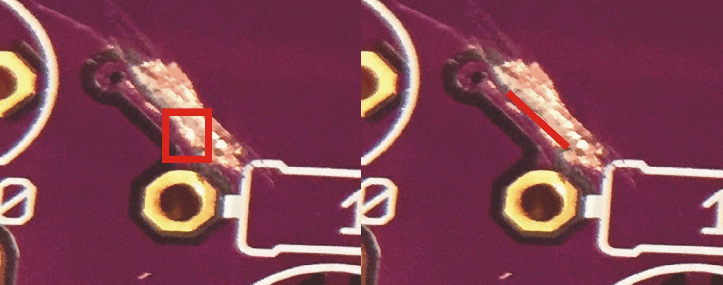
3. I still get continuity after the scrapping in this pic. Have I gone too far or not far enough? I would like to use this purple board instead of the green as it is a little easier to read.
This is the best focus I could get from my phone...

TIA!
John
I have been interested in putting together a HM for a while now, but I have been hesitant because a lot about this process is new to me. I saw that Bryan offered some the v4.2 BROKEN PCB. The ability to get a do-over, gave me enough confidence to give it a try. So, here I am at square one. I found the 4.2 Assembly album, another breakthrough at my level
Anyway, I am trying to follow Bryan's instructions on how to either cut the blue or cut the trace entirely.
I have a good 4.2 board, so I can test where I am not supposed to have continuity. I gave the scrapping a whirl, but I still get continuity. The instructions seem to be conflicting. One picture says to "Cut the trace entirely (both pad and via side) and run a wire to Q5". Yet the text on the product page says "Option 2: Cut the trace before the pad, and before it goes into the via (2 cuts) and run a wire to the lower pin of Q2 (just follow the trace)."
1. Does Q5 exist? I think that was a typo for Q2. Is there a way to test continuity on a good board?
2. TL;DR > Has anyone fixed one of these? A picture is worth a thousand words and it has taken me half that many to get to this point...
3. I still get continuity after the scrapping in this pic. Have I gone too far or not far enough? I would like to use this purple board instead of the green as it is a little easier to read.
This is the best focus I could get from my phone...
TIA!
John